NIKON INDUSTRIAL MICROSCOPES
Discover NIKON industrial microscopes with episcopic optical contrast inspection techniques in conjunction with digital imaging accessories for metallurgical material inspection in many industrial applications.
ECLIPSE L300ND, L300N and L200ND, L200N
Advanced Semiconductor Microscopes for Inspecting the Latest Fabrications
Superb Nikon CFI60-2 optics provide excellent images to both eyepieces and also to Nikon’s digital imaging cameras with analysis software. Combining these superior optics with an extraordinary illumination system delivers images of excellent contrast and resolution.
Nikon’s ECLIPSE L300ND, L300N and L200ND, L200NA is a range of semiconductor microscopes ideal for inspection of integrated circuits (IC), flat panel displays (FPD), large scale integration (LSI) electronic devices and many more applications.
Nikon ECLIPSE L300N(D) and L200N(D)
These microscopes are for exceptionally precise optical inspection of wafers (200mm for L200N series and 300mm for L300N series), reticles and other substrates.
Nikon CFI60-2 Optical Series
Nikon’s innovative design enables clear imaging techniques, including high contrast, brightfield, darkfield, polarization (POL), differential interference contrast (DIC) and double beam interferometry optical contrast.
Nikon Digital Sight Cameras
The full range of Nikon’s Digital Sight cameras efficiently captures images of a sample and deliver them to the image processing software of the NIS-Elements suite, together with microscope data on the objective lens used, magnification setting and light intensity.
Nikon CFI60-2 Optical Series
Nikon’s innovative design enables clear imaging techniques, including high-contrast, brightfield, darkfield, polarization (POL), differential interference contrast (DIC) and double beam interferometry optical contrast.
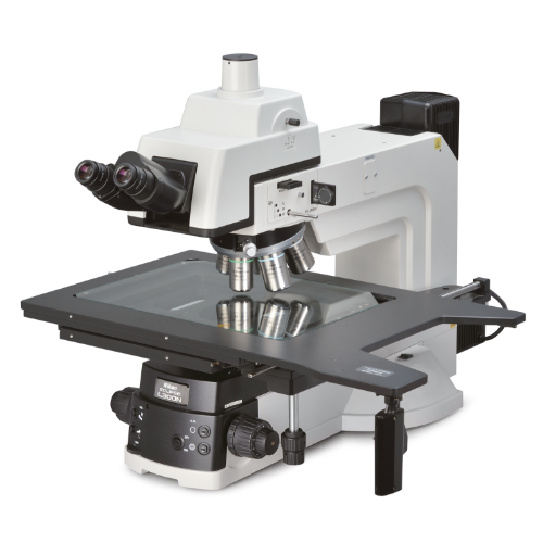
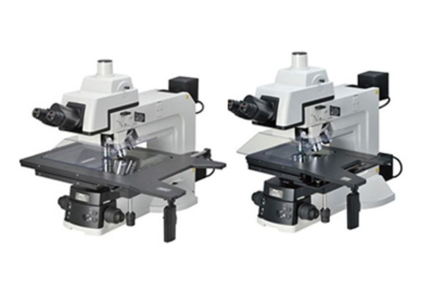
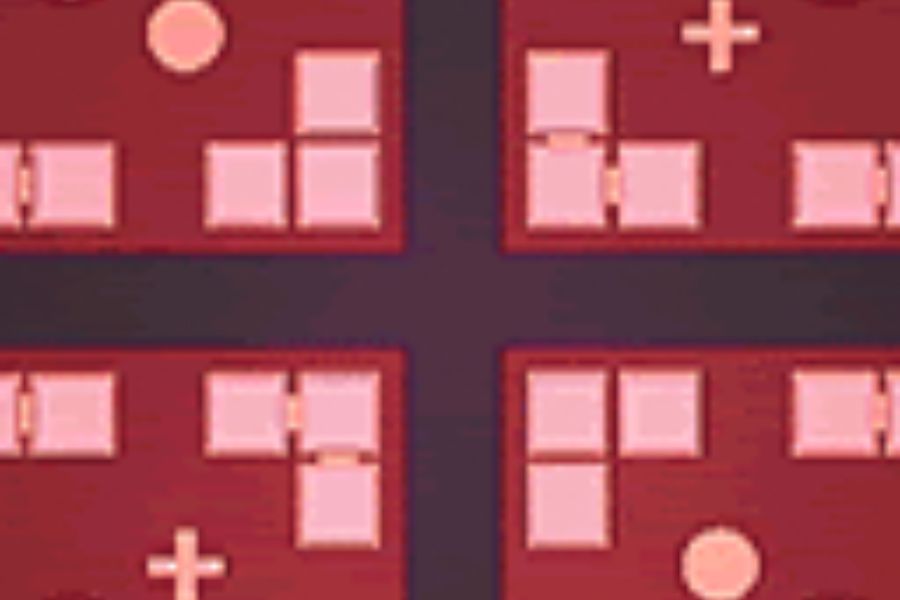
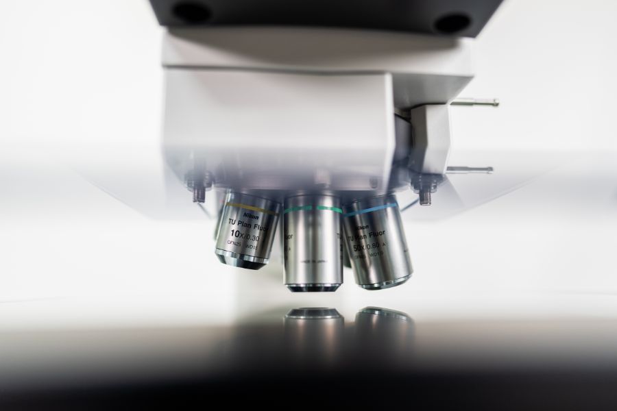
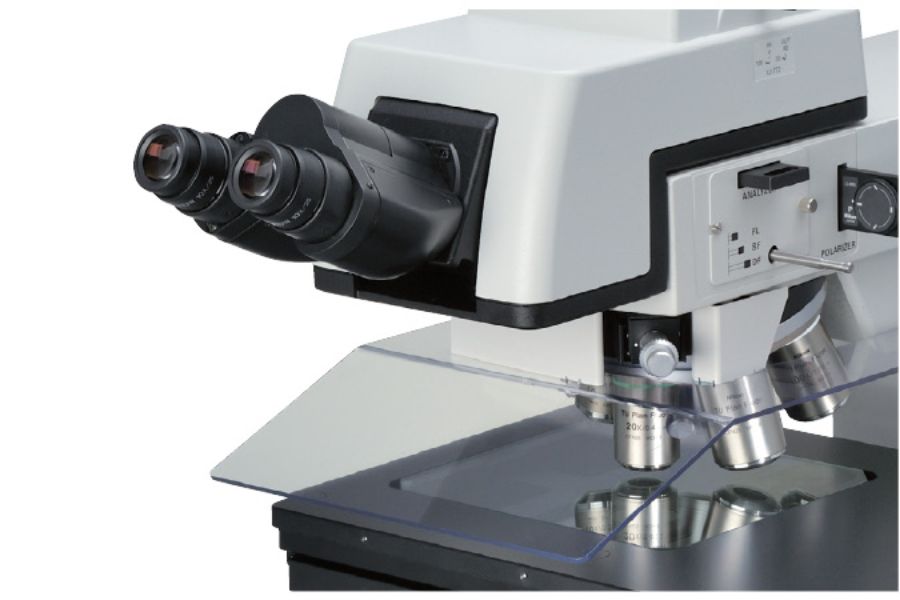
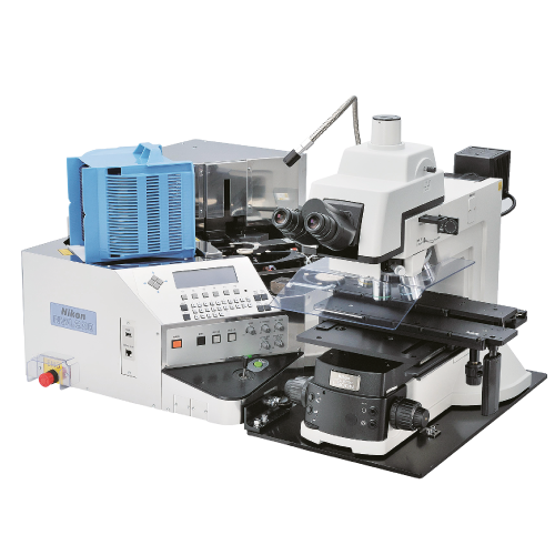
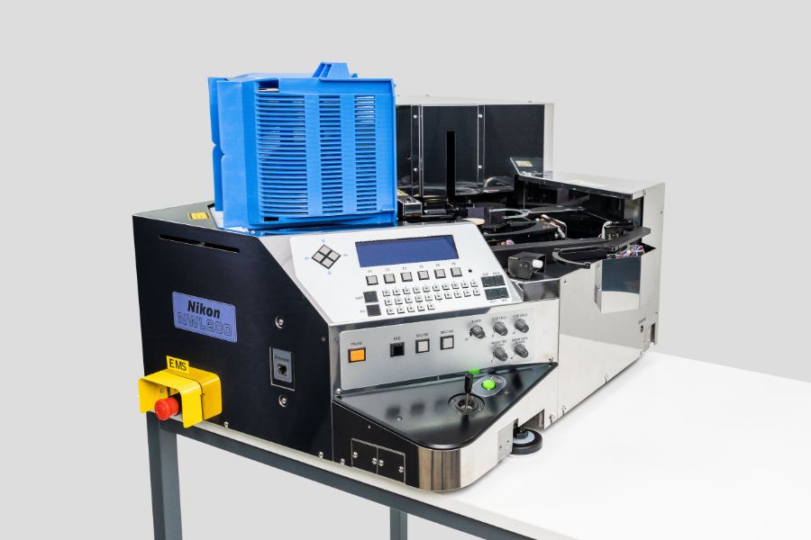
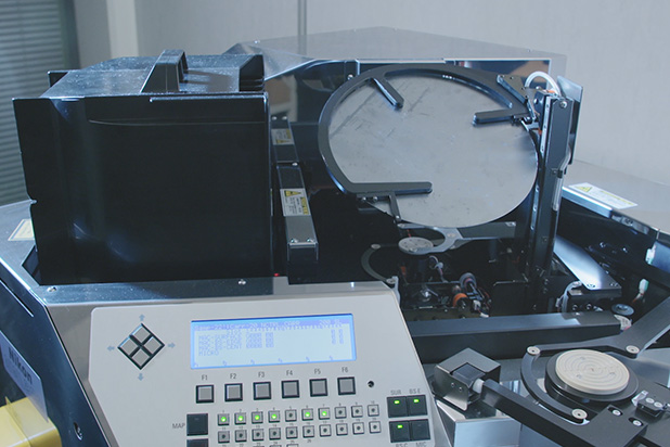
Universal Optical Contrast Methods
Reflected light: brightfield, darkfield, polarizing (POL), differential interference contrast (DIC), epi-fluorescence and two-beam interferometry. Transmitted light: brightfield, darkfield, polarizing, differential interference contrast and phase contrast.
Ergonomic Design Concept
Optimal positioning of operator controls and a variable angle eye-tube allows fatigue-free work. A right-way-up, right-way-around image is provided for correctly observing raw materials, semiconductors and industrial components.
Intelligent Digital Communication
The microscope detects and controls the objective lens in use, light intensity, episcopic illumination and aperture via a USB connection to Nikon’s NIS-Elements software.
NLW200 Wafer Loader Series
Sophisticated, Trusted Loader for Handling a Variety of Wafers
The NWL Series is a superb line-up of semiconductor wafer loaders from Nikon capable of transferring 6″ (150mm) and 8″ (200mm) diameter wafers down to a thickness of 100 microns (option) onto Nikon Eclipse L200N and LV150N microscopes or a NEXIV VMZ-S video measuring system.
High Reliability in Semiconductor Production
When the power supply is interrupted unexpectedly, the vacuum chuck of the macro arm remains active, allowing safe wafer removal.
Macro Inspection Functions
Semiconductor wafer front side pattern, back periphery and center area inspection is supported. The wafer rotation speed and tilt angle are set automatically or manually.